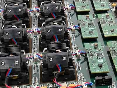
In the ever-evolving world of electronics, where performance demands are constantly pushing boundaries, ensuring the reliability of the fundamental building blocks – semiconductors – is paramount. This is where the often-overlooked process of burn-in comes into play.
Burn-in, in essence, is a rigorous testing methodology designed to stress semiconductors under controlled conditions, forcing potential weaknesses to surface before they can lead to catastrophic failures in the final product. This proactive approach significantly enhances the overall reliability of electronic devices, from the smartphones in our pockets to the complex machinery driving critical infrastructure.
This article delves into the intricate world of semiconductor burn-in, exploring its importance, various techniques, and the vital role KES Systems plays in providing industry-leading solutions for burn-in boards, burn-in systems, and cutting-edge wafer-level burn-in technology.
Why Burn-in Matters: Preventing Infant Mortality in Semiconductors
Imagine a scenario where a critical component in a medical device malfunctions. The consequences could be dire. Burn-in plays a crucial role in preventing such occurrences by weeding out potentially faulty semiconductors before they reach the end user. Here’s how:
- Early Failure Detection: Newly manufactured semiconductors can have inherent weaknesses that might not manifest under normal operating conditions. Burn-in exposes these chips to stress conditions, accelerating the emergence of such weaknesses, allowing for their identification and removal before they can cause problems in the field. This targeted approach helps manufacturers achieve a higher yield of reliable semiconductors. (See our article on The Bathtub Curve)
- Confidence in Reliability: By successfully undergoing burn-in, semiconductors demonstrate their ability to withstand demanding conditions. This provides manufacturers and, ultimately, end-users with increased confidence in the component’s long-term performance and reliability.
- Reduced Field Returns: A thorough burn-in process significantly reduces the likelihood of faulty components finding their way into finished products. This translates to fewer field returns, lower warranty costs, and a more positive brand reputation for manufacturers.
Reference: A detailed explanation of the benefits of burn-in testing can be found on the KES Systems website: https://www.kessystemsinc.com/solutions/
Demystifying Burn-in Techniques: A Multifaceted Approach
Burn-in isn’t a one-size-fits-all process. Different types of semiconductors require tailored approaches to effectively stress and test their functionalities. Here’s a look at some commonly used burn-in techniques:
- Static Burn-in: This method involves applying a constant voltage and current to the semiconductor while monitoring its behavior. It’s a simple and cost-effective approach, but it might not be sufficient for uncovering all potential weaknesses.
- Dynamic Burn-in: This technique uses a pre-defined set of test patterns to simulate real-world operating conditions. This puts the chip through its paces, pushing its performance limits and exposing potential flaws that static burn-in might miss.
- Temperature Cycling Burn-in: This approach subjects the semiconductor to repeated cycles of hot and cold temperatures, mimicking the thermal stresses experienced during normal operation. This helps identify weaknesses that might emerge due to thermal expansion and contraction.
Reference: For a more comprehensive overview of different burn-in techniques, refer to the JEDEC Solid-State Technology Association website: https://www.jedec.org/standards-documents
The Heart of the Process: Burn-in Boards and Systems
Burn-in boards are the foundation of the burn-in process. These specialized printed circuit boards (PCBs) serve as the platform upon which semiconductors are mounted and tested. (For more information on how to choose a burn-in board supplier, see our article here.)
KES Systems is a leading provider of high-quality, custom-designed burn-in boards. Their expertise lies in crafting boards that cater to a wide range of semiconductor types and application needs. Here’s what sets KES Systems apart:
- Customization: No two semiconductors are exactly alike. KES Systems understands this and offers a high degree of customization for their burn-in boards. They work closely with clients to ensure the boards perfectly match the specific requirements of the semiconductors being tested.
- High-Quality Materials: Burn-in boards operate under demanding conditions. KES Systems utilizes top-of-the-line materials and manufacturing processes to guarantee the boards can withstand these stresses, ensuring reliable and consistent test results.
- Advanced Features: KES Systems burn-in boards can be equipped with various advanced features, such as integrated power supplies, thermal management solutions, and data acquisition capabilities. This allows for comprehensive and efficient testing of various semiconductor functionalities.
Reference: To explore the vast range of burn-in board solutions offered by KES Systems, visit their website: kessystemsinc.com