by Bert Templeton
Abstract
The exigency for semiconductor reliability has reached unprecedented levels with the proliferation of advanced applications in automotive, aerospace, telecommunications, and medical technology. Burn-in testing remains a cornerstone in ensuring semiconductor longevity, serving as a preemptive measure against early-life failures by subjecting devices to elevated thermal and electrical stress conditions. This article provides a rigorous examination of burn-in methodologies, including High Accelerated Stress Testing (HAST) and High-Temperature Operating Life (HTOL) testing, and presents a critical analysis of the governing standards established by JEDEC, IEEE, IPC, and other regulatory bodies. Furthermore, this discourse underscores KES Systems’ preeminence in semiconductor burn-in solutions, delineating its technological advancements and commitment to elevating global semiconductor reliability benchmarks. Additionally, this study explores emerging trends in burn-in methodologies, the impact of evolving semiconductor architectures on testing requirements, and the role of data analytics and artificial intelligence in enhancing burn-in efficiency and defect detection rates.
Introduction
The relentless scaling of semiconductor technology, coupled with increasing functional integration and operational complexity, necessitates robust reliability assessment mechanisms. As semiconductor devices operate under diverse environmental and electrical stress conditions, premature failures pose significant risks to mission-critical applications. Burn-in testing has emerged as an indispensable reliability screening process, designed to precipitate latent defects and ensure only high-reliability components reach the field. This article delves into the technical underpinnings of burn-in testing, its indispensable role across various industries, and the pioneering contributions of KES Systems in advancing this domain. Furthermore, it explores the intersection of burn-in testing with machine learning, predictive analytics, and automated quality assurance to streamline reliability testing in modern semiconductor manufacturing.
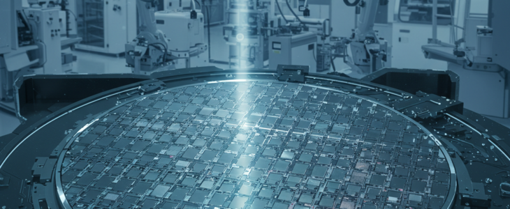
The Imperative of Burn-In Testing
Semiconductor Failure Mechanisms and the Need for Burn-In
Despite advancements in fabrication technologies, semiconductor devices remain susceptible to inherent defects arising from manufacturing process variations, material inconsistencies, and environmental stresses. Key failure mechanisms include:
- Electromigration: Gradual material transport due to high current densities
- Time-Dependent Dielectric Breakdown (TDDB): Progressive degradation of gate dielectrics
- Hot Carrier Injection (HCI): Charge trapping at semiconductor-dielectric interfaces
- Moisture-Induced Package Failures: Corrosion and delamination
- Bias Temperature Instability (BTI): Degradation of transistor threshold voltages over time
- Thermal Cycling Effects: Expansion and contraction-induced stress leading to interconnect fatigue
Burn-in testing proactively identifies these latent defects, ensuring long-term device reliability by precipitating failures in a controlled environment before deployment. Moreover, burn-in test optimization enables manufacturers to balance stress application and device longevity, mitigating unnecessary device degradation while ensuring effective failure screening.
Application Domains Demanding Semiconductor Reliability
Automotive Electronics
The transition toward autonomous and electric vehicles necessitates semiconductors that withstand extreme thermal and operational cycles. Automotive-grade components undergo stringent burn-in testing to comply with AEC-Q100 qualification standards, ensuring functional integrity under dynamic conditions. The integration of power electronics, sensors, and artificial intelligence into automotive platforms further amplifies the need for robust semiconductor reliability testing.
Aerospace and Defense
Avionic and defense-grade semiconductors operate in environments with extreme thermal fluctuations, radiation exposure, and high-vibration conditions. Compliance with MIL-STD-883 and other military reliability standards necessitates rigorous burn-in protocols. Moreover, advanced packaging technologies such as heterogeneous integration and chiplet-based architectures demand evolving burn-in methodologies to validate their resilience in extreme environments.
Medical Electronics
Medical devices, including implantable pacemakers and diagnostic imaging systems, require ultra-reliable semiconductors to mitigate catastrophic failure risks. Burn-in screening ensures adherence to stringent medical-grade reliability requirements. The emergence of bioelectronic interfaces and neural implants further necessitates advanced burn-in methodologies to ensure long-term biocompatibility and electronic stability.
Telecommunications and Data Centers
The exponential growth of cloud computing and 5G infrastructure necessitates semiconductors with superior thermal stability and endurance. Burn-in testing mitigates premature failures, ensuring uninterrupted high-performance computing and network operations. Moreover, optical interconnects and silicon photonics, increasingly adopted in high-speed data transmission, require novel reliability assessment techniques to prevent degradation in performance-critical applications.
Burn-In Testing Methodologies
High-Temperature Operating Life (HTOL) Testing
HTOL is a widely adopted accelerated stress test designed to evaluate long-term semiconductor reliability by exposing devices to sustained elevated temperatures and electrical stress. Key test parameters include:
- Temperature thresholds exceeding 125°C
- Continuous electrical bias application
- Test durations extending from hundreds to thousands of operational hours
This methodology facilitates the identification of intrinsic failure mechanisms such as TDDB, electromigration, and HCI, thereby enhancing predictive reliability modeling. Additionally, advancements in thermal management techniques are enabling higher test throughput and precision in stress application.
Highly Accelerated Stress Testing (HAST)
HAST is a specialized reliability assessment technique focusing on moisture-induced degradation of semiconductor packaging. This accelerated test method exposes devices to high humidity and temperature conditions to simulate real-world environmental stressors. Typical test conditions include:
- Temperatures reaching 130°C
- Relative humidity levels of 85% or greater
- Elevated electrical stress conditions
HAST is particularly instrumental in evaluating the robustness of encapsulation materials, interconnect reliability, and the effectiveness of moisture barrier coatings. Emerging approaches such as nano-coating technologies and hermetic sealing innovations are refining the scope of HAST and humidity resilience assessments.
KES Systems: Innovating the Future of Burn-In Solutions
Cutting-Edge Burn-In Technologies
KES Systems remains at the vanguard of burn-in technology, offering an extensive portfolio of advanced burn-in solutions. Key innovations include:
- High-power burn-in systems tailored for automotive and industrial-grade semiconductors
- Precision-engineered burn-in boards with superior thermal dissipation characteristics
- Customizable test sockets and interfaces optimizing electrical and thermal performance
- AI-driven burn-in analytics for predictive defect detection
Technological Advancements in Burn-In Methodologies
KES Systems continuously invests in next-generation burn-in solutions, integrating AI-driven analytics, thermal modeling, and real-time data acquisition to refine stress test methodologies. These advancements significantly enhance test efficiency, reduce power consumption, and improve defect detection accuracy. The incorporation of digital twin technology further augments the predictive modeling of failure mechanisms, allowing real-time optimization of burn-in test conditions.
Commitment to Regulatory Compliance and Quality Assurance
KES Systems aligns its burn-in solutions with the highest industry standards, ensuring conformance to JEDEC, IEEE, IPC, and other regulatory requirements. Its unwavering commitment to quality assurance and innovation solidifies its position as a trusted partner for semiconductor manufacturers worldwide.
Conclusion
Burn-in testing remains an essential reliability assurance methodology, underpinning the integrity of semiconductor devices across critical industries. By leveraging sophisticated stress test techniques such as HTOL and HAST, manufacturers can proactively identify latent defects, thereby mitigating field failure risks. KES Systems continues to redefine the landscape of semiconductor burn-in solutions, driving technological advancements that fortify semiconductor reliability and performance for next-generation applications. The integration of artificial intelligence, predictive analytics, and emerging packaging technologies will further enhance the effectiveness of burn-in testing, ensuring a resilient and high-performance semiconductor ecosystem for future applications.