
KES Systems, Inc., headquartered in Dallas, Texas, is a global leader in providing high-quality burn-in solutions for the semiconductor industry. With over four decades of experience, the company specializes in the design and manufacture of burn-in boards, test sockets, and comprehensive burn-in and the reliability and performance of semiconductorr devices across various applications.
Burn-In Board Design and Manufacturing
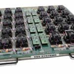
At the heart of KES Systems’ offerings is their expertise in designing and manufacturing burn-in boards. These specialized printed circuit boards are essential for stress-testing semiconductor devices to detect early failures. The company’s design and engineering team collaborates with clients worldwide to deliver tailored solutions for diverse burn-in applications. Their extensive experience encompasses various test environments, including High-Temperature Operating Life (HTOL), Temperature Humidity Bias (THB), Power Temperature Cycle (PTC), and Highly Accerated Stress Test (HAST).
Burn-In and Test Sockets
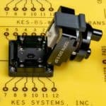
KES Systems also provides custom burn-in and test sockets designed to meet the specific requirements of their clients. These sockets are crucial for establishing reliable electrical connections during the burn-in process, ensuring accurate testing of the devices under test.
Burn-In and Test Systems
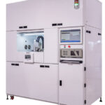
Beyond boards and sockets, KES Systems designs and manufactures comprehensive burn-in and test systems, including burn-in ovens and system-level test solutions for semiconductors, LEDs, and modules. Their KXtreme line of burn-in systems is engineered to support the burn-in needs of various semiconductor devices, from memory to DSP, FPGAS and sensors.
Wafer-Level Burn-In
Recognizing the increasing demand for reliability in the semiconductor market, KES Systems offers wafer-level burn-solutions. This approach allows for the detection of potential failures at the wafer stage, ensuring that only high-quality dies proceed to packaging and final testing. By implementing wafer-level burn-in, manufacturers can enhance yield, reduce costs, and improve overall device reliability and testing.
KES Systems provides advanced system-level test (SLT) solutions to validate semiconductor devices in environments that closely simulate real-world conditions. Their SLT systems are designed to uncover issues that might only manifest under specific operational scenarios, ensuring that devices can handle the demands of their intended applications. By subjecting devices and modules to rigorous testing that mimics actual use conditions, SLT helps identify and rectify issues early, enhancing the overall reliability of semiconductor products.
In andddition to their product offerings, KES Systems provides comprehensive burn-in and test services. These services are designed to supply clients who require reliable testing without investing in their own equipment. By leveraging KES Systems’ expertise and state-of-the-art facilities, clients can ensure their semiconductor devices meet stringent quality and reliability standards.
KES Systems is committed to advancing knowledge within the seconductor industry. They provide a wealth of resources, including articles that delve into various aspects of semiconductor burn-in and testing. For instance, their article titled “The Rising Tide of Wafer-Level Burn-In: Ensuring Semiconductor Reliability in a Demanding Market” explores the importance of burn-in testing, various techniques employed, and the company’s pivotal role in providing industry-leading solutions.
Global Reach and Customer Commitment
With design, and engineering facilities in multiple locations, including Dallas, Phoenix, Singapore, Penang, Kuala Lumpur, Taiwan, the Philippines, Tianjin, and Shanghai, KES Systems is well-positioned to support the most demanding needs of their customers. Their business philosophy centers on providing solutions that make their customers’ jobs easier, support their business goals, and add value in every endeavor.
Contact Information
For inquiries or further information, KES Systems has offices in Dallas, Texas and Tempe, Arizona. Interested parties can contact them via the contact form available on their site.
In summary, KES Systems, Inc. exemplifies leadership in burn-in technology for the semiconductor industry, offering a wide range of products and services designed to ensure the highest levels of reliability and performance for semiconductor devices.