Semiconductor devices, the tiny engines driving modern technology, undergo a fascinating transformation after their creation in fabrication plants (fabs). While the intricate dance of photolithography and etching breathes life into the intricate circuits on a silicon wafer, the journey is far from over. Semiconductor assembly takes these delicate “die” and transforms them into robust, functional packages ready to be integrated into electronic devices. This article dives deep into the world of semiconductor assembly, exploring the intricate processes, equipment, challenges, and future trends that define this crucial stage of chip creation.
The Assembly Line: Building a Secure Home for the Chip
Imagine a microscopic city rising on a silicon foundation. This is essentially what unfolds during semiconductor assembly. Here’s a breakdown of the key steps:
-
Die Attach: The fragile die is securely bonded to a leadframe, a metal frame with electrical connection points (leads). Techniques like epoxy bonding (using companies like Henkel AG & Co. KGaA (HEN3) for materials) or thermosonic bonding (utilizing equipment from companies like ASM International (ASML) and KLA Corporation (KLAC)) create a permanent, reliable connection.
-
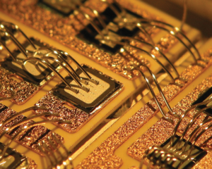
Wire Bonding: Ultra-thin wires, typically gold or copper, are used to establish electrical connections
 between the tiny bond pads on the die and the leads on the leadframe. High-precision wire bonders from companies like Kulicke & Soffa Industries (KLIC) perform this intricate task at incredible speeds. Industry standards like JEDEC JESD33B https://www.jedec.org/standards-documents/docs/jesd-59 define critical parameters for wire bonding, ensuring quality and reliability.
 -
Encapsulation: To shield the delicate die from physical damage and environmental threats, it’s encased in a protective material. Plastic mold compounds, often supplied by companies like Dow Chemical (DOW), are commonly used. Transfer molding machines from ASM International (ASML) precisely shape the plastic around the die, creating a robust package.
-
Trimming and Forming: Excess leadframe material is removed with laser cutting equipment from companies like IPG Photonics (IPGP) or Disco Corporation (6248:JP). The remaining leads are then formed into their final shapes for proper connection to the printed circuit board (PCB). Companies like Amkor Technology (AMKR) provide automated die trimming and lead forming equipment for this step.
-
Singulation: Individual packages are separated from the leadframe strip using high-precision sawing or laser cutting techniques. Companies like DISCO Corporation (DISCA) are major players in singulation equipment.
-
Final Cleaning and Marking: The completed packages undergo rigorous cleaning with equipment and chemicals from companies like Entegris, Inc. (ENTG) to remove any contaminants. Finally, laser marking equipment from companies like nLIGHT, Inc. (NLS) permanently inscribes identification codes and traceability information onto the package.
After assembly is complete, devices move on to various types of test including burn-in, HAST, and system level . KES Systems is a leading provider of solutions for all facets of these processes. For more information about KES Systems, please visit our contact page.