KES Systems: Expertise in Burn-In Technology and Semiconductor Testing
Introduction
In the rapidly evolving semiconductor industry, ensuring the reliability and performance of integrated circuits (ICs) is paramount. KES Systems stands at the forefront of this endeavor, offering unparalleled expertise in burn-in technology, system-level testing (SLT), wafer-level burn-in (WLBI), and advanced automation solutions. With a legacy of over four decades, KES Systems has become synonymous with quality and innovation in semiconductor testing solutions, continually pushing the boundaries of technology to improve efficiency and reliability.
Understanding Burn-In: A Crucial Process in Semiconductor Testing
Burn-in is a crucial reliability testing process where semiconductor devices are subjected to elevated temperatures and voltages to identify early-life failures. This process ensures that only the most reliable components progress to the next stages of production, thereby enhancing the overall quality of electronic devices.
KES Systems specializes in designing and manufacturing high-quality burn-in boards and systems tailored to meet the rigorous demands of modern semiconductor applications. Their expertise encompasses various facets of burn-in technology, including:
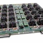
- Burn-In Boards: Custom-designed boards that facilitate the burn-in process by accommodating multiple devices under test (DUTs) simultaneously. These boards are optimized for thermal management, signal integrity, and longevity, providing consistent and accurate testing environments.
- Burn-In Systems: Comprehensive setups that integrate burn-in boards with environmental chambers, power supplies, and monitoring equipment to execute the burn-in process efficiently. KES Systems’ burn-in systems ensure precise temperature and voltage control, reducing the risk of failures in the field and increasing product lifespan.
- Burn-In Sockets: Specialized sockets that ensure secure and reliable connections between the DUTs and the burn-in boards during testing. These sockets are engineered to endure repeated thermal cycles and mechanical stress, offering long-term reliability and durability.
Wafer-Level Burn-In (WLBI) and Its Importance
Wafer-level burn-in (WLBI) is a critical testing process that enhances the reliability of semiconductor devices by detecting potential defects at the wafer stage. KES Systems provides advanced WLBI solutions that allow semiconductor manufacturers to screen devices before packaging, significantly improving yield rates and reducing post-manufacturing failures.

Benefits of Wafer-Level Burn-In:
- Higher Efficiency: Testing at the wafer level reduces handling and potential damage to individual chips, streamlining the manufacturing process.
- Cost-Effectiveness: Early defect identification minimizes waste and lowers costs associated with packaging faulty chips.
- Improved Reliability: Ensures that only fully functional chips proceed to final packaging, enhancing product performance.
KES Systems’ WLBI solutions support high-power and high-density semiconductor applications, catering to the evolving needs of the industry.
System-Level Test (SLT) and Its Role in Quality Assurance
System-level test (SLT) is a critical method for validating semiconductor devices under real-world conditions. Unlike traditional functional testing, SLT evaluates chips within an integrated environment to ensure they operate as expected in end-user applications.
Key Advantages of SLT:
- Comprehensive Functional Validation: Ensures chips function correctly in complete systems, reducing field failures.
- Detection of Latent Defects: Identifies issues that may not surface in standard functional tests.
- Enhanced Reliability Metrics: Assesses device performance under application-specific stress conditions.
KES Systems offers SLT solutions that integrate seamlessly with existing test platforms, providing manufacturers with reliable and scalable testing capabilities.
KES Expertise in Automation, Device Handling, and Burn-In Board Loading/Unloading
To streamline the burn-in process and improve efficiency, KES Systems has developed cutting-edge automation solutions for device handling and burn-in board loading/unloading. Their automated systems minimize manual intervention, reducing the risk of handling errors and ensuring consistent test conditions while also increasing throughput and reliability.
Key Features of KES Systems’ Automation Solutions:
- Automated Burn-In Board Handling: Reduces operator workload and increases throughput by seamlessly loading and unloading burn-in boards with precision.
- Robotic Device Placement: Ensures precise positioning of semiconductor devices, minimizing alignment errors and reducing mechanical stress on delicate components.
- Integrated Monitoring Systems: Real-time tracking of device handling parameters optimizes performance and reliability, reducing downtime and increasing overall production efficiency.
- Scalable Solutions: Designed to accommodate high-volume production environments and meet the evolving demands of semiconductor manufacturing.
By incorporating automation into burn-in testing, KES Systems helps manufacturers achieve higher efficiency, reduced operational costs, and improved test accuracy, ensuring that semiconductor devices meet the highest standards before reaching the market.
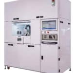
KES Expertise in MEMS Testing with the G32 Test Handler
KES Systems is a leader in MEMS (Micro-Electro-Mechanical Systems) testing, offering the G32 Test Handler as a high-precision solution for MEMS device validation. MEMS devices, used in applications such as automotive sensors, medical equipment, and consumer electronics, require stringent testing to ensure their functionality and reliability under real-world conditions.
Advantages of the G32 Test Handler:
- High-Precision Handling: Ensures accurate positioning and alignment of MEMS devices during testing, reducing the risk of measurement inaccuracies.
- Multi-Site Testing: Enables concurrent testing of multiple MEMS devices, significantly increasing throughput and reducing testing times.
- Environmental Control: Supports temperature and humidity-controlled testing, ensuring MEMS devices operate reliably under a variety of conditions.
- Flexible Test Configurations: Adaptable for various MEMS device types, including accelerometers, gyroscopes, and pressure sensors, making it an ideal solution for diverse MEMS applications.
With the G32 Test Handler, KES Systems delivers an industry-leading MEMS testing solution that enhances device reliability, increases testing efficiency, and meets the rigorous demands of the MEMS industry.
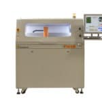
KES Klean Contact System for Burn-In Board and Socket Cleaning
Over time, burn-in boards and sockets accumulate debris and contamination, affecting test accuracy and device reliability. KES Systems addresses this challenge with the Klean Contact System, an advanced cleaning solution designed to maintain optimal contact performance, extending the longevity of testing equipment.
Key Features of the Klean Contact System:
- Automated Cleaning Process: Removes oxidation, debris, and contaminants from burn-in boards and sockets efficiently and consistently.
- Non-Abrasive Cleaning Technology: Protects delicate components while ensuring thorough cleaning, preventing damage during maintenance.
- Improved Electrical Contact Reliability: Reduces contact resistance and enhances test signal integrity, ensuring more accurate and reliable test results.
- Extended Equipment Lifespan: Reduces wear and tear on burn-in boards and sockets, minimizing maintenance costs and extending the usability of testing equipment.
By utilizing the Klean Contact System, semiconductor manufacturers can achieve consistent test results, prolong the life of their testing equipment, and reduce downtime associated with manual cleaning, ensuring continuous and reliable production operations.
Global Presence and Commitment to Excellence
With offices in Dallas, Phoenix, Singapore, Malaysia, Taiwan, the Philippines, and China, KES Systems is well-positioned to serve the needs of both small and global companies. Their superior support, cutting-edge technology, and commitment to innovation in burn-in technologies and services have made them a trusted partner in the semiconductor industry.