Imagine a world where every smartphone, car, or medical device works flawlessly, no matter the conditions. At the heart of that reliability lies a critical process called burn-in board design, and KES Systems, Inc., a cornerstone of the Sunright Group, is writing the story of its success. For over 40 years, KES Systems has been the world’s leading creator of burn-in boards, those unsung heroes that ensure semiconductors—from microprocessors to sensors—can handle the toughest real-world challenges. With a global reach spanning Dallas to Shanghai and a client list boasting nine of the top ten semiconductor giants, KES Systems weaves innovation, precision, and trust into every burn-in board they design and manufacture. Let’s dive into their journey, exploring how their expertise in burn-in board design shapes industries like automotive, aerospace, and beyond, all while keeping semiconductor reliability at the forefront.
Why Burn-In Board Design Matters in Today’s Electronics
Picture a printed circuit board (PCB)—a intricate web of copper tracks and pads that brings electronic devices to life. PCBs are the backbone of everything from your smartwatch to a jet’s navigation system, connecting components to make technology hum. But in the semiconductor world, there’s a special kind of PCB called a burn-in board, designed to test chips under extreme conditions like scorching heat or high voltages. This process, known as burn-in or burn in, roots out weak components before they reach you, ensuring only the strongest survive.
Creating these burn-in boards isn’t easy. They need to maintain crystal-clear signals, manage blistering temperatures, and stay tough through countless test cycles. That’s where burn-in board design comes in, blending science and artistry to craft boards that perform flawlessly under pressure. KES Systems has mastered this craft, producing burn in boards that help semiconductors shine in applications from self-driving cars to life-saving medical devices. Their burn-in board design expertise ensures every chip is ready for the real world, making them a trusted partner in the electronics saga.
KES Systems: A Story of Innovation in Burn-In Board Design
KES Systems’ tale began over four decades ago, when they set out to perfect burn-in board design. Today, as part of Sunright Limited—listed on the Singapore Exchange since 1994—they tap into the global might of the Sunright Group, the world’s largest provider of burn-in and test services. From their hub in Dallas, Texas, to facilities in Phoenix, Singapore, Penang, Kuala Lumpur, Taiwan, the Philippines, Tianjin, and Shanghai, KES Systems tells a story of connection, serving clients across automotive, telecommunications, computing, medical, aerospace, and photonics.
Their mission? To make life easier for their customers, aligning with their goals and delivering value through every burn-in board they create. KES Systems’ portfolio is a rich tapestry, weaving together burn-in boards, ATE test boards, system-level test (SLT) systems, burn-in ovens, custom test sockets, and wafer-level burn-in (WLBI) solutions. At the heart of it all is their unparalleled burn-in board design, a blend of technical brilliance and collaborative spirit that has earned them the trust of industry titans and rising stars alike. Their work in burn in technology is more than a service—it’s a legacy of reliability.
Crafting Excellence: KES Systems’ Burn-In Board Design Expertise
Step into KES Systems’ design studio in Dallas, where a team with over 100 years of combined experience brings burn-in board design to life. These engineers are storytellers, using advanced tools to craft burn in boards that range from simple two-layer FR4 designs to intricate multilayer, flex, and rigid-flex creations made with high-temperature, high-speed laminates. Every burn-in board they design is a chapter in a larger narrative of semiconductor reliability, tailored to meet the unique needs of each client.
The Art of Custom Burn-In Board Design
Imagine designing a burn-in board that’s perfect for a specific chip, whether it’s a tiny sensor or a powerful processor. KES Systems does just that, creating burn-in boards that fit like a glove, handling various package types, pin setups, and stress conditions. These boards are built for efficiency and durability, thriving in tests like High-Temperature Operating Life (HTOL), Temperature Humidity Bias (THB), Power Temperature Cycle (PTC), and Highly Accelerated Stress Test (HAST). Their burn-in board design ensures crystal-clear signals, steady temperatures, and electromagnetic harmony, making them the go-to choice for platforms like MCC, Delta-V, Aehr, Eles, Despatch, Hirayama, and KES Systems’ own KXtreme burn-in systems.
High-Speed and High-Voltage Burn-In Board Design
Some chips are speed demons or powerhouses, and KES Systems’ burn-in board design rises to the challenge. For high-speed digital or high-voltage applications, their engineers support 0.3mm pitch BGAs and beyond, using tools like BoardSim to fine-tune layouts. They tame issues like overshoot, undershoot, impedance mismatches, and crosstalk, ensuring burn in boards perform flawlessly. In high-voltage scenarios, they guard against Cathode Anode Filament (CAF) and Electrochemical Migration (ECM), crafting burn-in boards that endure the toughest tests.
Component Library and BOM Analysis for Burn-In Boards
Every great story needs the right characters, and in burn-in board design, that’s the components. KES Systems maintains a robust component library, checking parts, validating accuracy, and ensuring availability. Their Bill of Materials (BOM) analysis is like editing a script, balancing cost and performance by validating CAD/schematic data and suggesting alternative parts. This meticulous approach makes their burn in boards both reliable and cost-effective, keeping the narrative smooth from design to production.
PCB Fabrication and Design for Manufacturability (DFM)
Building a burn-in board is like constructing a stage—it has to be perfect for the performance. KES Systems conducts PCB fab checks, examining signal and power integrity, crosstalk, drill specs, and solder mask/silkscreen details to ensure their burn-in board design translates seamlessly to manufacturing. Their Design for Manufacturability (DFM) analysis catches potential hiccups early, boosting yields and cutting costs for burn in boards, all rooted in decades of industry know-how.
PCB Assembly and Stencil Check for Burn-In Boards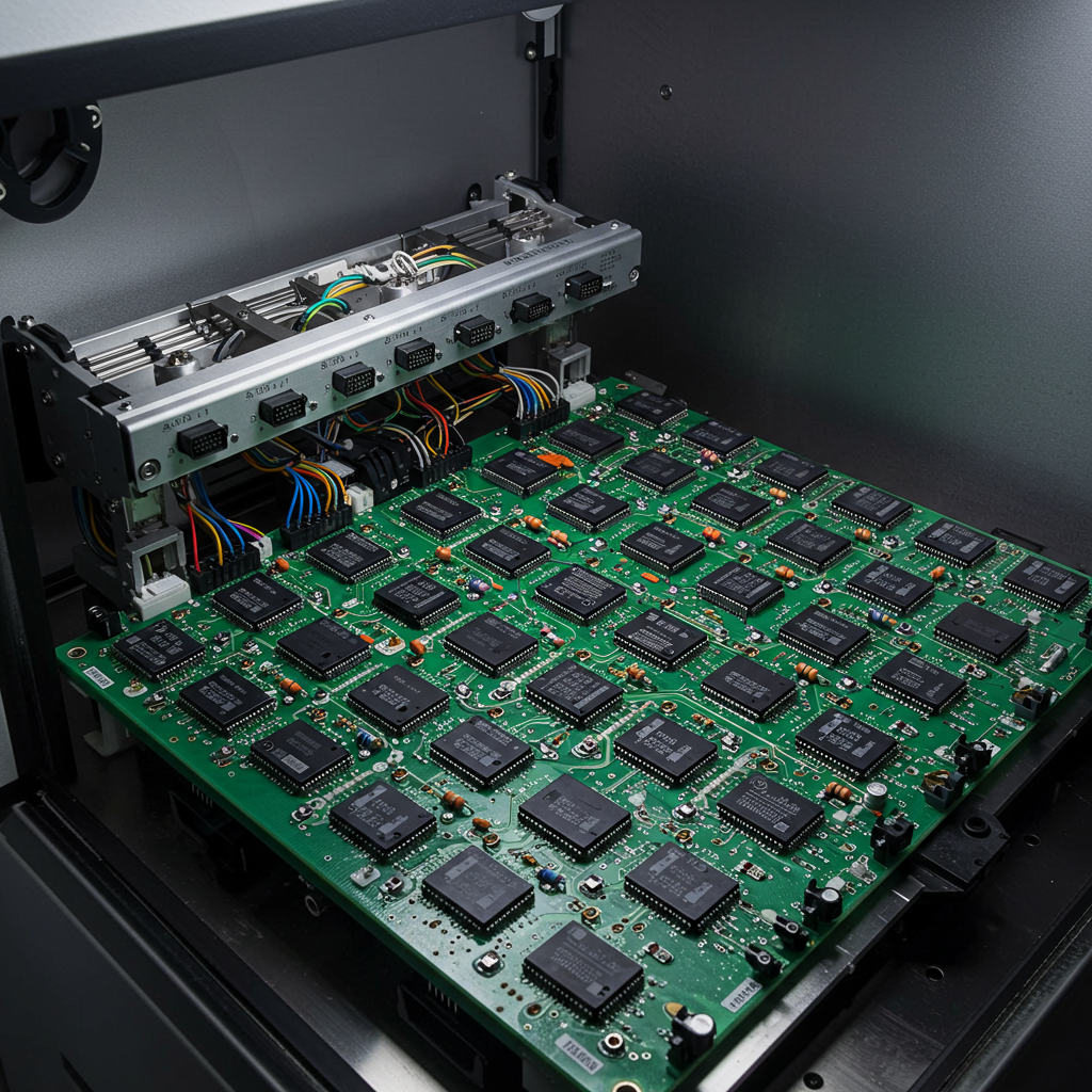
Assembling a burn-in board is like choreographing a dance—every step matters. KES Systems validates footprint/pad dimensions, stencil openings, spacing, and soldering parameters to ensure smooth assembly. Their stencil design expertise ensures precise solder paste application, vital for strong joints on burn in boards. For complex setups like Ball Grid Arrays (BGAs), they perfect alignment and soldering, keeping defects at bay.
Thermal Analysis in Burn-In Board Design
Heat is a villain in burn-in testing, but KES Systems’ burn-in board design turns it into a manageable character. Using tools like TASPCB Harvard, they map heat buildup, optimizing power and ground planes to keep burn in boards cool and prevent hotspots. This thermal storytelling ensures their boards thrive in the fiery conditions of burn-in testing.
3D Mechanical Simulation and Modeling
Some burn-in boards face physical stress, like actors on a demanding set. KES Systems uses Pro E for 3D mechanical simulation, analyzing flex and external forces during loading and unloading. This ensures their burn in boards remain resilient, ready for the rigors of burn-in testing.
CAD/Gerber Source and Net Compare
Every burn-in board design starts with a blueprint, and KES Systems supports Cadence 17.4/16.6, generating Gerber files and drill outputs. Their netlist comparison tools act like proofreaders, verifying integrity and producing detailed summaries. Features like shed CAD port, duplicate CAD ports, sorted test reports, and net compare summaries add depth to their burn in board narrative, ensuring accuracy.
HAST and THB Burn-In Board Design
For tests like HAST and THB, KES Systems writes a careful script, preventing issues like CAF and ECM in their burn-in board design. They maximize air gaps, follow IPC-2221 spacing standards, and ensure post-assembly cleanliness, crafting burn in boards that excel in humid, high-pressure conditions. Their compression mount sockets support high-density and high-voltage devices, adding reliability to the burn-in story.
Automotive and Specialized Burn-In Board Design
The automotive world, with its Battery Electric Vehicles (BEVs), Advanced Driver Assistance Systems (ADAS), and battery management systems, demands top-tier burn-in board design. KES Systems delivers, creating burn in boards that meet strict standards. Their expertise also shines in medical, military, aerospace, industrial automation, and photonics, where burn-in boards must perform under extreme conditions, ensuring every chapter ends with reliability.
A Collaborative Approach to Burn-In Board Design
KES Systems’ burn-in board design process is a partnership, starting with a deep dive into customer needs during the request for quote (RFQ) phase. Their engineers guide clients on laminate choices, trace spacing, and component placement, shaping burn in boards that balance performance and manufacturability. Quick-turn design services speed up prototyping for new product introductions (NPIs), while their knack for complex burn-in board design on tight deadlines makes them a trusted ally worldwide.
Building the Story: Manufacturing Burn-In Boards
KES Systems doesn’t just design burn-in boards—they bring them to life with world-class manufacturing. Their facilities hum with advanced equipment, weaving precision and quality into every burn in board they produce, from one-off prototypes to high-volume runs.
Crafting Burn-In Boards with Precision
Creating a burn-in board is like building a masterpiece. KES Systems’ fabrication process tells a detailed story:
-
Inner Layer Fabrication: Etching patterns onto copper-clad laminates with photoresist and UV exposure.
-
Layer Lamination: Stacking layers with prepreg material, fused under heat and pressure.
-
Drilling and Copper Plating: Crafting vias and mounting holes, plated for conductivity.
-
Outer Layer Imaging and Etching: Defining circuits and clearing excess copper.
-
Solder Mask and Surface Finish: Adding protective masks and finishes like ENIG, HASL, or immersion tin.
-
Silkscreen Printing: Marking legends and details.
This process creates multilayer burn-in boards, flex circuits, and rigid-flex designs, tackling the toughest test challenges.
Surface Mount Technology (SMT) Line for Burn-In Boards
KES Systems’ SMT line is the stage where burn-in boards come alive, supporting 0402 and 0201 components, fine-pitch BGAs, and high-pin-count connectivity. The cast includes:
-
Automatic Screen Printer: Applies solder paste with precision.
-
Pick and Place Machines: Position components flawlessly.
-
Reflow Oven: Uses convection reflow and vapor phase machines for high-mass burn in boards, forging strong connections.
-
Automated Optical Inspection (AOI): Spots flaws like misalignment or solder issues.
-
Selective Soldering Machine: Targets through-hole parts delicately.
-
Wave Soldering Machine: Handles traditional soldering.
-
Solder Paste Inspection (SPI): Checks paste quality.
-
BGA Rework Station: Fixes complex packages.
-
Flying Probe Testing: Ensures electrical integrity.
-
KIC Reflow Monitoring: Perfects reflow profiles.
-
Conformal Coating: Shields burn-in boards with a pouring method for HAST/HTOL burn-in, protecting against moisture and corrosion.
Producing Burn-In Boards for Every Platform
As the world’s top burn-in board manufacturer, KES Systems crafts burn in boards for all major test platforms, built to withstand 200°C temperatures, high voltages, and endless thermal cycles. Their burn-in boards support multi-DUT testing, boosting efficiency and cutting costs.
Custom Sockets for Burn-In Boards
Every burn-in board needs a supporting cast, and KES Systems’ custom test sockets deliver. Designed for burn in boards and ATE boards, these sockets ensure secure connections, reliability, and minimal stress, handling non-standard packages and high-density burn-in testing with ease.
Ensuring Quality in Burn-In Boards
Quality is the climax of KES Systems’ story. Their burn-in boards undergo electrical testing, signal integrity checks, thermal analysis, and visual inspections, meeting ISO certifications and IPC standards. The Klean Contact System, a proprietary cleaning solution, extends burn in board life by reducing contact resistance and contamination, ensuring high yields.
Turnkey Solutions for Burn-In Boards
KES Systems offers a full turnkey experience, weaving together burn-in board design, socket integration, assembly, and burn-in testing. This seamless narrative shortens time-to-market. With a maximum PCB size of 800mm x 700mm, they support large-scale burn in boards, while flexible lines handle high-mix, low-volume production for NPIs.
Specialized Manufacturing for Automotive and High-Reliability Burn-In Boards
In fields like automotive, medical, and aerospace, burn-in boards face high stakes. With over 30 years of experience, KES Systems crafts burn in boards for:
-
Battery Management Systems: Thriving in high-voltage settings.
-
ADAS Sensors: Performing under extreme conditions.
-
Avionics and Military Systems: Built tough for rugged use.
-
Medical Devices: Ensuring reliability in critical equipment.
Their processes perfect high solder barrel fill, selective soldering, and high/low-temperature capabilities, making burn-in boards both durable and high-performing.
Beyond Burn-In Boards: Comprehensive Testing Solutions
KES Systems’ story doesn’t end with burn-in board design. They offer a full suite of burn-in and test solutions, using their global reach and technical expertise to support clients at every step.
Burn-In Boards and Systems
KES Systems’ burn-in boards set the industry standard, handling multiple DUTs across diverse test environments. Their KXtreme burn-in systems pair burn in boards with environmental chambers, power supplies, and monitors, controlling temperature, voltage, and parameters with precision. These systems support everything from memory to processors, sensors, and FPGAs.
Wafer-Level Burn-In (WLBI)
Wafer-level burn-in (WLBI) catches flaws early, boosting yield and cutting costs. KES Systems’ WLBI burn-in boards are designed for density and efficiency, perfect for high-volume production.
System-Level Test (SLT) Solutions
Their SLT systems, like the Tiger module test handler, mimic real-world conditions to validate performance. Using robust burn in boards, these systems support engineering, pre-production, and high-volume testing, ensuring reliability.
Burn-In Services
For clients needing flexibility, KES Systems’ burn-in services deliver scalable, reliable testing worldwide. Tailored to specific needs, these services rely on advanced burn-in boards to keep the story moving forward.
Automation and MEMS Testing
KES Systems is a trailblazer in automation and MEMS testing, offering:
-
Automated Burn-In Board Handling: Speeds up testing and eases workloads.
-
Robotic Device Placement: Positions DUTs perfectly on burn in boards.
-
Integrated Monitoring Systems: Tracks performance in real-time.
These solutions enhance accuracy, cut costs, and streamline burn-in board applications.
Impacting Industries with Burn-In Board Design
KES Systems’ burn-in board design is a game-changer, touching lives across industries:
-
Automotive: Powering BEVs, ADAS, powertrain control, and battery management with reliable burn in boards.
-
Telecommunications: Supporting 5G, networking, and wireless communication with high-speed burn-in boards.
-
Computing: Driving servers, data centers, and high-performance systems with robust burn in boards.
-
Consumer Electronics: Enabling smartphones, gaming consoles, and wearables with compact burn-in boards.
-
Medical Devices: Ensuring diagnostic and therapeutic equipment reliability with burn in boards.
-
Aerospace and Defense: Building rugged burn-in boards for avionics and military systems.
-
Industrial Automation: Fueling robotics and control systems with durable burn-in boards.
Serving nine of the top ten semiconductor companies, KES Systems’ burn-in board design fosters innovation, writing success stories across electronics.
A Real-World Tale: Automotive Semiconductor Testing
In the automotive world, BEVs and ADAS rely on flawless chips. KES Systems’ burn-in board design supports high-voltage battery management systems and sensor-rich ADAS platforms, meeting tough standards. Their burn in boards ensure safety and performance, helping drive the future of electric and autonomous vehicles.
Innovation and Quality at the Heart of Burn-In Board Design
Innovation is KES Systems’ muse, fueling their burn-in board design with heavy investments in research and development. Their engineers explore new materials, techniques, and automation, pushing burn in board performance forward. Recent chapters include:
-
Klean Contact System: Prolongs burn-in board life by reducing contact resistance and contamination.
-
High-Power Burn-In Solutions: Supports LEDs and power semiconductors with sturdy burn in boards.
-
Advanced Automation: Boosts throughput and precision in burn-in board testing.
Quality is their promise, woven into every burn-in board through ISO certifications, IPC standards, and rigorous checks. Using top-tier materials from Isola, Arlon, and Rogers, plus component derating and thermal management, they ensure burn in boards last.
Sustainability in Burn-In Board Manufacturing
KES Systems tells a green story, embracing sustainability in burn-in board production. By reducing waste, optimizing energy, and extending product life, they align with eco-friendly electronics trends, ensuring their burn in boards leave a positive legacy.
The Future of Burn-In Board Design
The PCB world is ever-changing, and KES Systems’ burn-in board design is ready to lead:
-
High-Density Interconnect (HDI) Burn-In Boards: Enabling compact devices with finer lines and microvias.
-
Flexible and Rigid-Flex Burn-In Boards: Supporting innovative designs.
-
Embedded Components: Enhancing burn in board performance within layers.
-
3D Burn-In Boards: Opening new integration possibilities.
-
Advanced Materials: Using superior properties for burn-in boards.
-
Sustainability: Prioritizing eco-friendly burn in board processes.
With innovation and scalability, KES Systems crafts burn-in board design for tomorrow’s electronics.
KES Systems, Inc. is more than a company—it’s a storyteller, weaving reliability into the fabric of electronics through burn-in board design. Their 40-year journey has made them a global leader, creating burn-in boards that ensure semiconductor excellence for industries from automotive to aerospace. As part of the Sunright Group, they draw on a worldwide network and deep expertise to drive burn-in innovation, serving the top semiconductor players with burn in boards that stand the test of time.
With a passion for innovation, quality, and partnership, KES Systems is shaping the future of burn-in board design. From burn in boards that guarantee chip reliability to testing solutions that streamline production, they’re writing the next chapter for the devices that power our world.