
Understanding High Voltage Burn-In Testing
High-voltage burn-in testing is a critical quality assurance process for identifying defects in semiconductor devices before they reach consumers. The burn-in process involves subjecting devices to elevated temperatures and voltages, accelerating potential failures and allowing manufacturers to weed out weak components early in their lifecycle.
Importance of Burn-In Testing
Burn-in testing serves several essential purposes:
- Reliability Assessment: It helps ensure that semiconductor devices can withstand operational stresses without failure.
- Defect Identification: By exposing devices to extreme conditions, manufacturers can identify latent defects that may not be apparent under normal operating conditions.
- Yield Improvement: Effective burn-in processes can increase yields by ensuring that only reliable products are shipped.
The burn-in process typically involves applying voltages that are 30% higher than the maximum operational voltage and maintaining temperatures between 95°C to 105°C for varying durations, depending on device specifications
Types of Semiconductor Devices Requiring High-Voltage Burn-In
Specific semiconductor devices are particularly suited for high-voltage burn-in testing due to their applications in demanding environments. Notable examples include:
Silicon Carbide (SiC) Devices
Silicon Carbide is known for its high thermal conductivity and ability to operate at high voltages and temperatures. SiC devices are commonly used in:
- Power Electronics: These include converters and inverters for renewable energy systems.
- Electric Vehicles (EVs): SiC transistors improve efficiency and reduce thermal management requirements.
High-voltage burn-in testing for Silicon Carbide (SiC) devices presents several specific challenges:
- Threshold Voltage Instability: SiC MOSFETs exhibit V<sub>TH</sub> instability, leading to current distribution imbalances in parallel-connected devices. This instability can cause some devices to switch on earlier, potentially overloading and damaging them.
- Thermal Management: SiC devices operate at higher temperatures, making it challenging to maintain consistent temperatures across all devices during burn-in testing
- Extended Stress Testing: Due to higher extrinsic failure rates, SiC devices require longer and more rigorous burn-in tests, especially for automotive applications.
- Unique Failure Mechanisms: Traditional silicon-based testing protocols are insufficient for SiC, as these devices have distinct material properties and operational stresses
- Higher Voltage Requirements: SiC devices are designed for higher voltage operations, necessitating burn-in systems capable of applying and controlling these elevated voltages safely
- Conductivity Modulation: For high-voltage SiC bipolar devices, the conductivity modulation effect in thick voltage-blocking layers presents challenges in optimizing on-resistance and switching speed
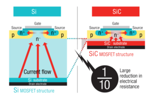
- Die Size and Heat Dissipation: SiC devices have smaller die sizes than silicon equivalents, which can cause heat dissipation issues during burn-in testing.
- Packaging Strain: The smaller die size of SiC devices can result in increased packaging-related strain during the burn-in process
To address these challenges, manufacturers are developing specialized burn-in systems and protocols tailored to the unique properties of SiC devices, including wafer-level burn-in testing to improve cost-effectiveness and reliability screening.
The leading causes of threshold voltage instability in SiC MOSFETs are:
- The high density of interface states: SiC MOSFETs have a significantly higher density of interface states compared to Si devices, which affects the threshold voltage stability
- Near-interfacial oxide traps (NIOTs): Also known as border traps, these contribute to threshold voltage instability through charge trapping and de-trapping mechanisms
- Carrier injection: Under bias stress, electrons, and holes can tunnel into traps near the SiC/SiO2 interface, causing threshold voltage shifts.
- Pre-existing traps: Short-term charging and discharging of traps located near or at the SiC/gate-oxide interface contribute to threshold voltage dynamics during switching
- Large bandgap of SiC: The wide bandgap leads to significant thermal emission barriers, allowing trapped charges to remain at the interface for extended periods, keeping the device in a non-equilibrium state
- Bipolar gate switching: The application of positive and negative gate voltages during regular operation causes recurring threshold voltage variations due to charge trapping and de-trapping
These factors combine to create a complex threshold voltage instability issue in SiC MOSFETs, which requires careful consideration in device design and application.

Bias-stress significantly affects the threshold voltage (V<sub>TH</sub>) in SiC MOSFETs through several mechanisms:
- Near-interface oxide traps (NIOTs): Bias-stress causes injection of carriers into NIOTs by direct tunneling, leading to V<sub>TH</sub> shifts
- Polarity-dependent shifts: Positive gate bias tends to increase V<sub>TH</sub>, while negative gate bias decreases it
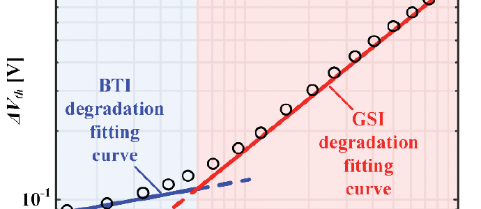
- Time-dependent behavior: V<sub>TH</sub> shifts follow a power law with stress time, with an exponent (n) ranging from 0.03 to 0.09, depending on stress temperature and level.
- Temperature effects: The magnitude of V<sub>TH</sub> drift varies with temperature, showing smaller drift at higher temperatures but with changing slope
- Reversibility: Unlike in silicon devices, V<sub>TH</sub> shifts in SiC MOSFETs are nearly fully reversible via negative gate bias and do not cause permanent interface damage
- Cyclic behavior: Short-term V<sub>TH</sub> variations recur in every switching cycle, representing an inherent device characteristic rather than degradation.
- Hysteresis: SiC MOSFETs exhibit V<sub>TH</sub> hysteresis during gate voltage sweeps, with the magnitude depending on sweep range and speed
These effects are attributed to charge trapping/de-trapping in pre-existing oxide defects rather than creating new defects.
Understanding these bias-stress impacts is crucial for accurately predicting device behavior and reliability in various applications.
Challenges in High Voltage Burn-in Testing
Despite its importance, high-voltage burn-in testing presents several challenges:
- Thermal Management: It is crucial to maintain consistent temperatures across all devices, but this can be difficult due to variations in package sizes and materials.
- Voltage Regulation: Ensuring stable voltage levels during testing is essential to avoid damaging sensitive components.
- Testing Time: Balancing thorough testing with production schedules can lead to bottlenecks if not appropriately managed.
KES Systems’ Solutions
KES Systems has established itself as a leader in addressing the complexities associated with high-voltage burn-in testing through a range of innovative solutions:
Custom Burn-In Boards
KES Systems designs and manufactures custom burn-in boards tailored to specific device requirements. Their boards are engineered for maximum density and cost-efficiency, ensuring effective stress testing while minimizing space requirements.
Advanced Burn-In Systems
The company provides comprehensive burn-in systems that integrate automation and handling capabilities. These systems are designed to maintain tight control over thermal environments, ensuring that all devices receive uniform treatment during tests.
Expertise and Support
With over 40 years of experience, KES Systems offers unmatched expertise in semiconductor burn-in processes. They provide consultation services on the latest materials and technologies, helping clients optimize their testing strategies. Their commitment to quality ensures that all products meet rigorous industry standards.
Comprehensive Testing Solutions
Beyond burn-in boards, KES Systems offers various services, including system-level tests, cleaning solutions for burn-in boards, and ongoing maintenance support. This holistic approach ensures that clients have access to everything they need for effective semiconductor testing.