Semiconductor burn-in is a method for detecting early failures in semiconductor devices. This is also called, ‘infant mortality’. It requires the testing of devices under a set of stress conditions that usually involves an elevated temperature of 125° C to 150° C (commonly, some ‘high reliability” device can be tested at 200° C or higher) for a set number of hours.
During that time the devices have a voltage applied to its power inputs, known as biasing the part. If no additional stimulation is applied it is known as static burn-in. If the device is stimulated with digital and/or analog inputs, the device must be monitored to know when and if the device fails. This is known as monitored or dynamic burn-in. The temperature, length of time and other conditions are usually governed by a set of standards, or agreement with the end-user of the device.
Burn-in testing attempts to weed out failures from stage 1 of the “bathtub” curve for the reliability of electronics, which gives the failure rate vs. time plot of electronic components.
!EMPTY!
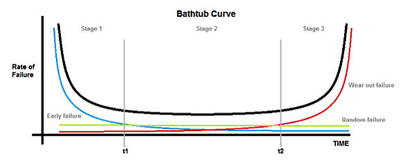
This curve has three stages:
- Stage 1: Infant Mortality/Early Life – This is the period were early failures show up in a component. These are due to a lack of control in manufacturing processes at the molecular level. During this period components fail at a high rate but this rate decreases with time. (Curve in blue shows failure rate due to early fails)
- Stage 2: Normal/Useful Life – This is the period where the rate of failure is nearly constant, and due to randomly occurring faults. (shown with the green curve)
- Stage 3: Wear Out/End of Life – Period marked by an increase in failure rate due to the aging of components; this period marks the end of the useful life span of a device. These failures are due to critical paths in the device getting worn out. (Curve in red shows failure rate due to aging).
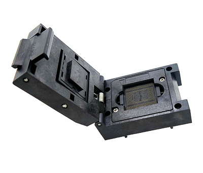
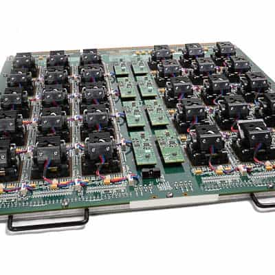
In order to perform this test, devices are loaded into sockets on a specifically made burn-in board. These sockets can be loaded manually, or with an autoloader, such as a product from the KES FastTrack line of autoloaders.
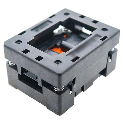
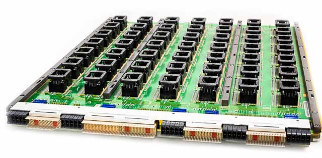
Photo credit: Bert Templeton
Once the devices under test (DUTs) are loaded into the sockets on the burn-in board, the board or boards are put into a burn-in system specifically for those boards and applications. There are many types of burn-in systems for semiconductors. KES makes a variety of systems to accommodate devices from 4 pins to over 1,000 pins. And for devices that dissipate less than 1W to over 100W. The specific systems will also have a number of power supplies to supply the various voltages used on modern devices. These can range from a few millivolts to over 100V, and from a few milliwatts to over 500A.
In addition to power supplies, the burn-in systems are capable of providing multiple I/O to stimulate, measure and monitor the DUTs during the burn-in process. Your KES representative can work with you to determine the proper system, board, and programming needed for your device.
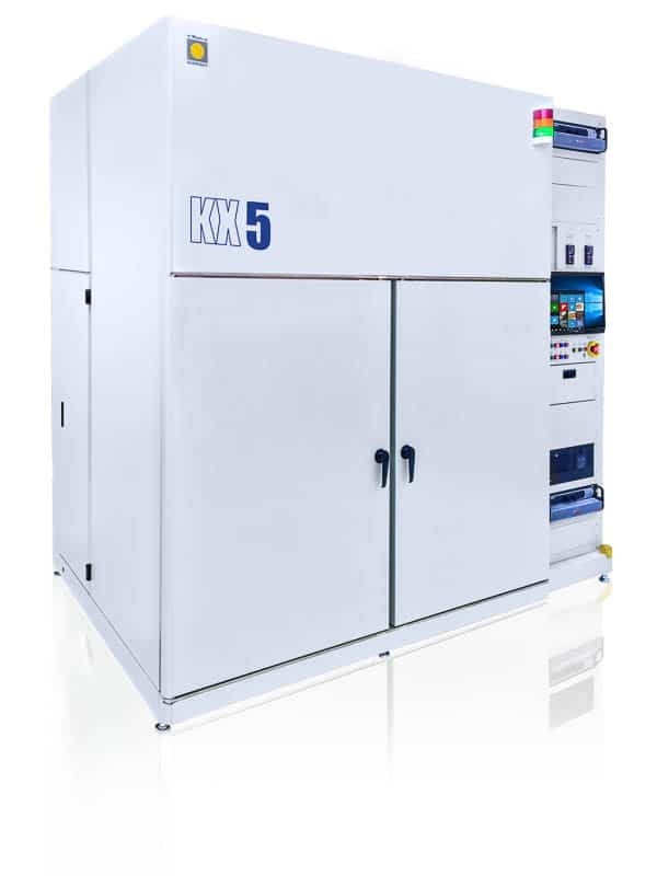
Once the boards are loaded into the burn-in system, specific test programs are run on those boards and devices to stress, test and evaluate there condition to the specified requirements. This will include factors such as temperature (either chamber temperature, DUT package temperature, or device junction temperature), voltage(s), digital patterns to be run to stimulate the devices, and parameters to monitor for pass/fail conditions.
Once the testing has completed, logs of every device are generated for sorting the pass/fail devices after burn-in.
In addition to traditional semiconductor burn-in, another common reliability test for semiconductors is HAST. See our introduction to HAST testing, and HAST board design guidelines for more information on HAST.
For more information about burn-in applications and how KES can help you and your team achieve your objectives, please contact us and we will be glad to help. We have over 40 years of solving complex burn-in and reliability testing for the semiconductor industry.
KES Systems is a member of the Sunright family of companies, providing products and services to the industry for more than 40 years.
